Nano-devices, materials and fabrication research
Electronic properties and quantum physics of graphene nanostructures
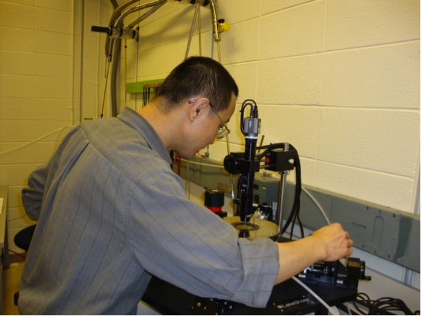
Dr. Zhixian Zhou's group studies the electronic properties and quantum physics of graphene nanostructures with the purpose of developing carbon-based nanoelectronics.
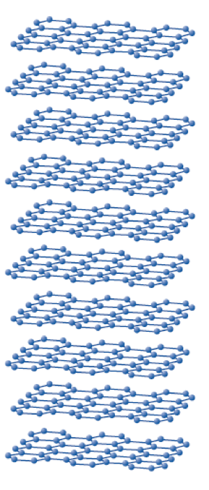
Graphene consists of a single layer of graphite. It features superior electrical, thermal and mechanical properties:
- Electrons can move several hundred times faster in graphene than in silicon.
- Graphene conducts heat over 10 times faster than copper.
- Graphene is about 100 times stronger than steel.
Graphene is, therefore, a very attractive material that can be potentially utilized in many areas. Examples of prospective applications are touch screens, solar cells, fast transistors, gas sensors and lightweight super strong materials as pointed out by Professor Per Delsing in his Presentation Speech for the 2010 Nobel Prize in Physics.
Dr. Zhou's group has recently obtained record high mobility in suspended graphene nanoribbons (GNRs), observed Intrinsic bandgap in ultraclean GNRs, attained experimental evidence of magnetism in chiral GNRs and achieved high on/off ratio in suspended GNRs.
Recent publications on graphene nanoribbon research
Ming-Wei Lin et al., Room-Temperature High On/Off Ratio in Suspended Graphene Nanoribbon Field Effect Transistors, Nanotechnology 22, 265201 (2011).
Ming-Wei Lin et al., Approaching the Intrinsic Bandgap in Suspended High-Mobility Graphene Nanoribbons, Phys. Rev. B 84, 125411 (2011).
Cheng Ling et al., Electrical transport properties of graphene nanoribbons produced from sonicating graphite in solution, Nanotechnology 22 325201 (2011).
Quantum transport in one-dimensional GaAs systems
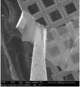
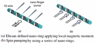 The goal of this ongoing experiment is to realize an ultra-dilute 1D hole system in a single mode wire in GaAs HIGFET and detect the charge and spin correlation of 1D holes with a charge pump. It consists of nanofabrication processes to implement the charge and spin pumps next to the quantum wire [figure]. The pumping effect is detected by measuring the differential conductance as a function of the pumping frequencies.
This setup is a first-time realization of the Thouless charge pump that operates by adiabatically pushing charges with a moving external periodic potential while the Fermi level of the holes lying in a mini gap opens up due to the Bragg diffraction.
Restricted by the gap, the electron system is dragged by a traveling potential wave in a conveyor-belt fashion, resulting in a pumped quantized current in the 1D channel in the units of electron charge times the wave frequency. The enhanced electron-electron interaction should increase the mini gaps due to the Bragg diffraction, enhancing the adiabaticity.
Two and one-dimensional electron systems in graphene
Graphene is an authentic two-dimensional layer of carbon atoms that exhibits extraordinary mechanical, thermal, optical and electrical properties. Though during the past five years, graphene research has undergone rapid expansion, the methods of effectively handling such thin atomic layers and means of application remain to be explored.
Following the scotch tape method and gating within the substrate, the realization of suspending single layers has led to suppressed disorder. Recently, in addition to the integer quantum Hall effect, the fractional quantum Hall effect has just been reported. With a charge density of 3x1011cm-2, we almost enter into a fascinating regime where the electron-electron interaction dominates, a fundamentally important subject that has never been explored in systems with linear dispersion relation.
The new class of quantum charge and spin phenomena arising from the correlation effect has become promising. The following describes some graphene research ideas that are closely related to the 2D study I have done in ultra-high purity strongly correlated GaAs and Si semiconductor systems.
Our focus is to fabricate of high-quality electron systems in graphene and perform transport measurement. Even with the suspension techniques, the fabrication of graphene still suffers from the impurity invasion during clean fabrication (i.e., in-situ) in addition to the preexisting disorder. The problem becomes serious since a typical single graphene is roughly ten microns in size and the processes such as making Ohmic contact results in pollution through diffusion of metal particles.
One solution is to have a large enough area so that the contact leads, which can be sacrificially polluted by disorder, are separated from the sample area.
We are currently developing a soft method to produce large graphene sheets followed by an in-situ sublimation method. The transferring of the graphene is realized with nanomanipulators and transfer the graphene with the tip of the manipulator onto substrates.
This work is carried out in collaboration with Dr. JY Huang at CINT at Sandia National Labs.
For more information, please see Dr. Jian Huang's research.