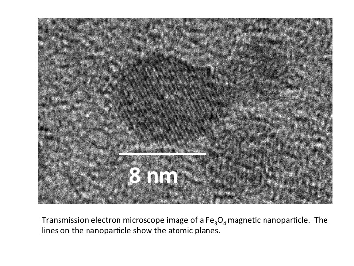
Magnetism and magnetic materials research
 Our research program in magnetic materials focuses on the fabrication and property characterization of magnetic thin films and the development of these materials for device and sensor applications.
Of particular interest are studies of domain structures in single-layered ferromagnetic thin films, multilayer structures exhibiting giant magnetoresistance, spin-polarized magnetic tunnel junctions and hybrid semiconductor/ferromagnetic devices. Characterizations are primarily focused on transport (magnetoresistance and I-V characteristics) and magnetic (SQUID magnetometry, vibrating sample magnetometry, ac susceptometry and ferromagnetic resonance) measurements between liquid helium and room temperature.
Additionally, magnetic force microscopy is utilized to determine the local magnetic structures of sub-micron-size features and a point conductance technique based on the Andreev reflection of electrons has been developed for measuring the spin polarization of ferromagnetic materials. Magnetic films and devices are fabricated by molecular beam epitaxy (MBE), electron-beam and sputter deposition systems. This program also makes extensive use of the facilities and research collaborations associated with the interdisciplinary Smart Sensor and Integrated Microsystems program.
Spin polarization mapping
This research focuses on the implementation of nanoscale spin polarization measurements utilizing Micro Electro Mechanical Systems (MEMS) positioning technology in combination with electroforming of three-dimensional (3D) microstructures.
A simple new technique of electrodeposited (ED) photoresists makes possible conformal coatings of highly structured surfaces and, when combined with electroplating, can form new types of advanced 3D metal microstructures. By developing an array of micro-tips integrated with through-wafer interconnects into a single testing chip, individually addressable m × n arrays of microscopic superconducting tips on a testing chip can be fabricated.
Then, this testing chip will be applied to thin films and planar magnetic nanostructures to map the spin polarization over a larger cross-section and will allow non-destructive device evaluation at any stage of the device fabrication. Furthermore, since both electrodeposition and electroplating processes have the ability of forming complex topographies, this technique has the potential to develop other 3D metallic microstructures for other potential applications.